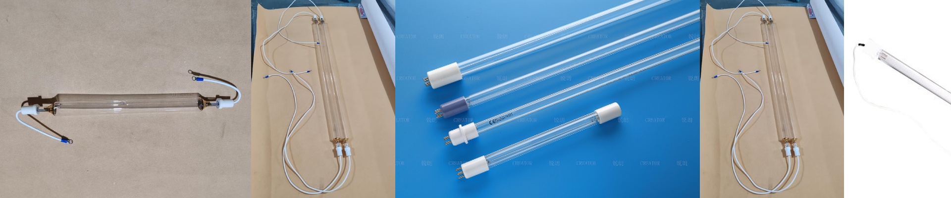
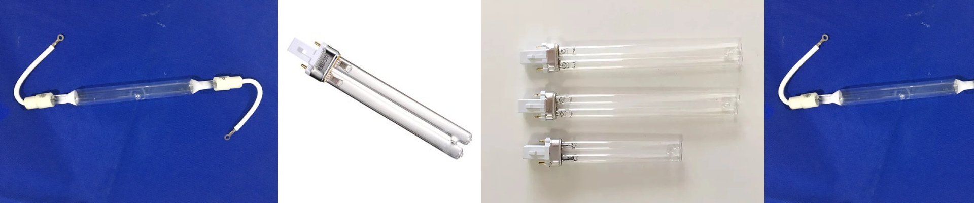
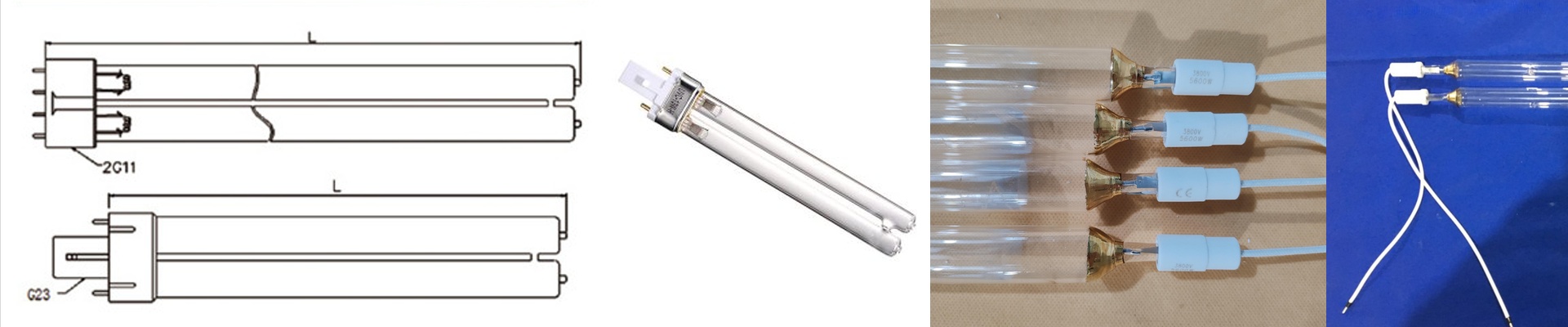
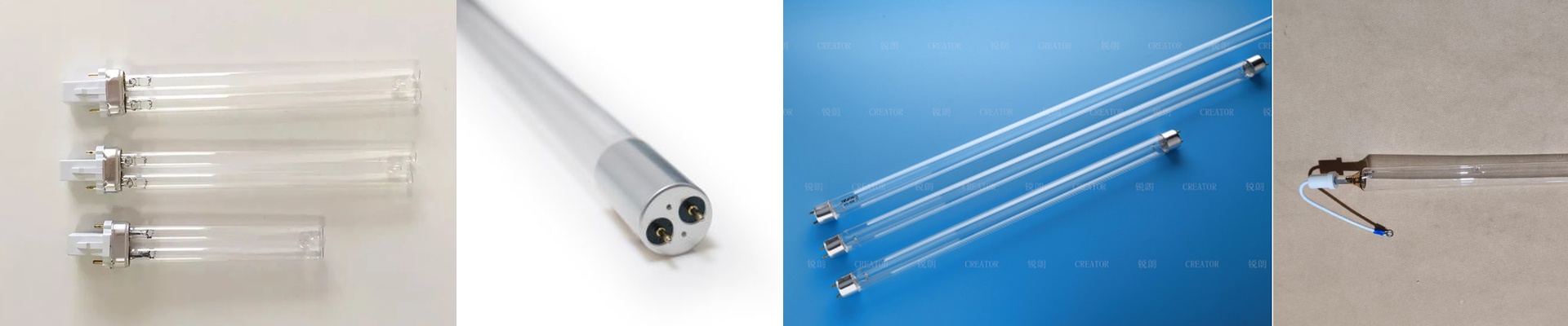
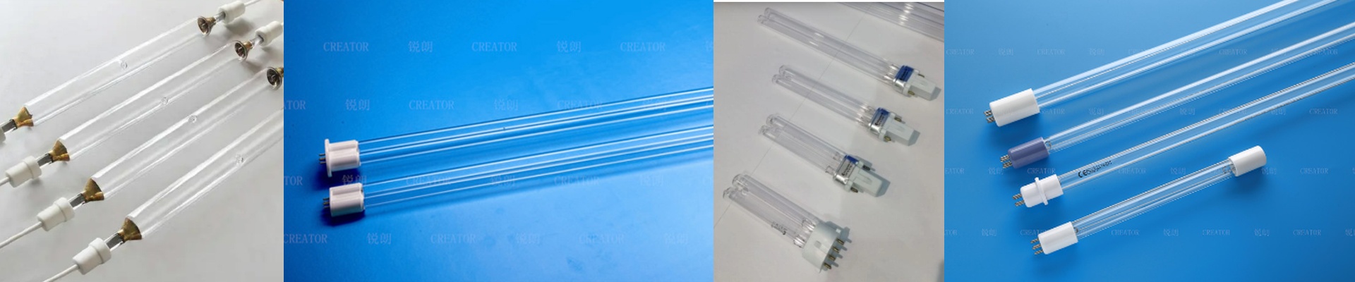
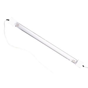
Out on the fab floor, the clock after wafer dicing ticks in seconds, not minutes. UV-tape debonding is where you either protect yield or throw it away—too much cure leaves adhesive behind; too little and you get chip fly-away. What you need is a UV source that repeats the same spectral output and energy density, cycle after cycle. What actually matters technically Semiconductor tapes rely on photoinitiators that are tuned to specific UV bands, usually 365 nm and 385 nm. We run lamps with narrow-band emission, using dichroic reflectors to keep the broadband IR from dumping heat into the wafer. Peak irradiance at the substrate plane tops 2.5 W/cm², which gives you over 2,000 mJ/cm² of curing energy in under 10 seconds. Output stays within 3% stability over 3,000 hours, and the lamp stays ozone-free thanks to a quartz envelope built for high UV transmission. Why this works in practice Dicing tapes are engineered for rapid cross-linking. When the lamp spectrum matches the photoinitiator absorption, you get an instant surface cure while the bulk adhesive stays intact—so the tape strips clean, in one piece. The payoff is faster throughput: cycle time drops from 30 seconds to under 10, without thermal stress on thin-film structures. You end up with consistent peel force, fewer rejects, and lamp replacement that lines up with scheduled maintenance. The details that bite you Alignment has to be dead-on. Even 2 mm of defocus can cut effective irradiance in half. Put an inline radiometer on the line and measure dose at the substrate, not just lamp power. The lamp runs at low thermal load, but the fixture still needs forced air cooling to hold reflector temperature steady—otherwise spectral consistency drifts and reflector life drops. Plan for 24 V control integration, and double-check connector compatibility with your handler.